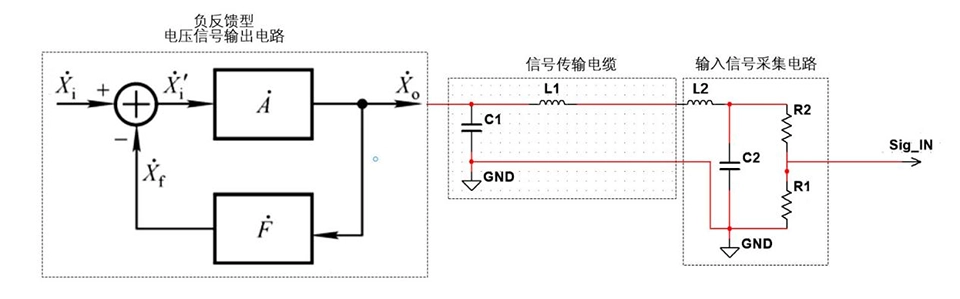
Fig. 1 Transmission path of voltage source signals
As shown in Fig. 1, the transmission of the voltage source signal consists of 3 main parts:
Negative feedback type voltage signal output circuit.
Signal transmission cable. Among them, C1 and L1 are the parasitic capacitance and parasitic inductance of the cable, whose parameters are directly related to the cable length and wiring type.
Input signal acquisition circuit. Wherein, L2 and C2 are low-pass filtering circuits that may be arranged for some of the sampling circuits.
For a negative feedback type voltage signal output circuit, the input signal is calculated as follows:
∣Xi′∣=∣Xi∣-∣Xf∣
When the phase of ∣Xf∣ overshoots or lags by 180°, the formula for the input signal takes the following form:
∣Xi′∣=∣Xi∣+∣Xf∣
In other words, in the absence of an input signal (∣Xi∣ is 0), the feedback signal (∣Xf∣) maintains the output signal (|X0|), and the output signal (|X0|) in turn maintains the feedback signal (∣Xf∣). At this point, self-excited oscillation is formed.
In summary, the following 2 conditions are the prerequisites that lead to self-excited oscillations:
|AF| > 1
φA+φF=(2n+1)Π
Where does the phase difference on the loop come from?
Parasitic C1 and L1 on the signal transmission cable, L2 and C2 on the input signal acquisition circuit, and filter capacitance on the signal output circuit may cause phase differences in advance or lag. The final phase difference is the sum of these phase differences, and if it is 180° over- or lagged, self-excited oscillation is possible.
How can self-excited oscillations be avoided?
We just need to make sure that the previous 2 conditions cannot be satisfied simultaneously in the range of the applied frequency domain to avoid self-excited oscillations.
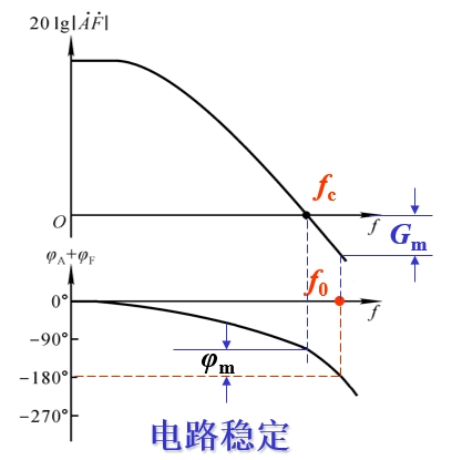
Fig. 2 Condition of negative feedback loop without oscillation
As in Figure 2:
f c is the frequency at which the loop gain 20log|AF| drops to 0 dB.
f o is the frequency at which the loop phase difference is less than -180°.
Therefore, the circuit is stable when the phase difference overshoots or lags by 180° and the gain of the loop drops below zero.
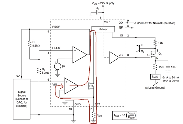
Why are current source signals relatively less prone to oscillation?
Fig. 3 Current source feedback loop
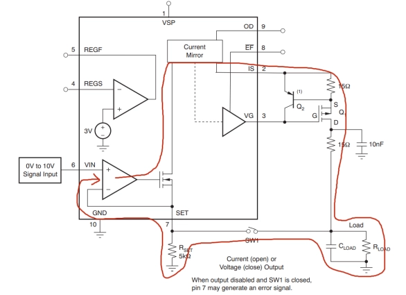
Fig. 4 Voltage source feedback loop
As shown in Fig. 2, the output of the current source, which is widely used today, is a mirror current source. Its negative feedback regulation loop contains only one side of the mirror current source identified by the red line. Therefore, the external load circuit has little influence on the phase difference and gain of the feedback loop, and as long as the parameters of the internal feedback loop are controlled, no oscillation will occur.
As shown in Figure 3, the feedback point for the voltage source signal is located at the output point of the circuit. Therefore, the feedback loop contains the internal circuit marked by the red line and the external cable and sampling circuit. Thus, when the electrical parameters of the external cable or sampling cable change, the phase difference and gain of the negative feedback loop also change. When this change causes the 2 conditions for self-excited oscillation to be satisfied, oscillation occurs.


 Egong.com.cn 42018502006527 No.